Publisher: Supplier of LED Display Time: 2022-09-28 11:33 Views: 2380
High-power LED packaging has been a research hotspot in recent years due to its complex structure and process, which directly affects the performance and life of LED displays, especially high-power white LED packaging. Next, the editor of LCF will give you a detailed introduction to what is high-power LED packaging technology?
The functions of the LED package mainly include:
1. Mechanical protection to improve reliability;
2. Strengthen the heat dissipation to reduce the junction temperature of the wafer and improve the performance of the LED;
3. Optical control, improve light output efficiency and optimize beam distribution;
4. Power supply management, including AC/DC conversion, and power control.
The selection of LED packaging methods, materials, structures and processes is mainly determined by factors such as wafer structure, optoelectronic/mechanical properties, specific applications, and cost. After more than 40 years of development, LED packaging has gone through development stages such as bracket type (Lamp LED), SMD type (SMD LED), and bare core type LED (COB LED).

Key technologies of high-power LED packaging
High-power LED packaging mainly involves light, heat, electricity, structure and technology. These factors are both independent of each other and affect each other. Among them, light is the purpose of LED packaging, heat is the key, electricity, structure and technology are the means, and performance is the specific embodiment of the packaging level. In terms of process compatibility and reducing production costs, LED package design should be carried out at the same time as chip design, that is, the package structure and process should be considered during chip design. Otherwise, after the wafer is fabricated, the structure of the wafer may be adjusted due to packaging requirements, thereby prolonging the product development cycle and process cost, and sometimes even impossible.

Low thermal resistance packaging process
For the existing LED light efficiency level, since about 80% of the input electrical energy is converted into heat, and the LED chip area is small, the chip heat dissipation is a key problem that must be solved in LED packaging. It mainly includes chip layout, packaging material selection (substrate material, thermal interface material) and process, heat sink design, etc.
LED package thermal resistance mainly includes internal thermal resistance and interface thermal resistance of materials (heat dissipation substrate and heat sink structure). The function of the heat dissipation substrate is to attract the heat generated by the wafer and conduct it to the heat sink to achieve heat exchange with the outside world. Commonly used heat dissipation substrate materials include silicon, metals (such as aluminum, copper), ceramics (such as Al2O3, AIN, Sic), and composite materials. For example, Nichia's third-generation LED uses CuW as the substrate, and flip-chips a 1mm chip on the CuW substrate, which reduces the thermal resistance of the package and improves the luminous power and efficiency; Lamina Ceramics has developed a low-temperature co-fired ceramic metal substrate. , and developed the corresponding LED packaging technology. This technology firstly prepares a high-power LED chip and a corresponding ceramic substrate suitable for eutectic welding, and then directly welds the LED chip and the substrate together. Because the eutectic solder layer, electrostatic protection circuit, driving circuit and control compensation circuit are integrated on the substrate, it is not only simple in structure, but also has a high thermal conductivity of the material and few thermal interfaces, which greatly improves the heat dissipation performance, which is a high-power LED array package. A solution is proposed. The high thermal conductivity copper clad ceramic board developed by German Curmilk company is made of ceramic substrate (AIN and Al2O3) and conductive layer (Cu) sintered under high temperature and high pressure. No binder is used, so it has good thermal conductivity, high strength and insulation. powerful. Among them, the thermal conductivity of aluminum nitride (AIN) is 160W/mk, and the thermal expansion coefficient is 4.0×10⁻⁶/℃ (equivalent to the thermal expansion coefficient of silicon, which is 3.2×10⁻⁶/℃), thereby reducing the thermal stress of the package.
Studies have shown that the package interface also has a great influence on thermal resistance. If the interface cannot be handled correctly, it is difficult to obtain a good heat dissipation effect.
High light extraction rate package structure and process
During the use of LEDs, the loss of photons generated by radiative recombination when emitted outward mainly includes three aspects: internal structural defects of the wafer and absorption of materials; reflection losses of photons at the exit interface due to refractive index differences; The total reflection loss caused by the incident angle greater than the critical angle of total reflection. Therefore, a lot of light cannot be emitted from the wafer to the outside. By coating a transparent adhesive layer (potting adhesive) with a relatively high refractive index on the surface of the wafer, since the adhesive layer is located between the wafer and the air, the loss of photons at the interface is effectively reduced, and the light extraction efficiency is improved. In addition, the role of the potting compound includes mechanical protection of the wafer, stress relief, and as a light guide structure. Therefore, it is required to have high light transmittance, high refractive index, good thermal stability, good fluidity and easy spraying. In order to improve the reliability of LED packaging, the potting compound is also required to have the characteristics of low moisture absorption, low stress, and aging resistance. Currently commonly used potting compounds include epoxy resin and silicone. Because of its high light transmittance, high refractive index, good thermal stability, low stress and low hygroscopicity, silicone rubber is obviously superior to epoxy resin and is widely used in high-power LED packaging, but the cost is high. Studies have shown that increasing the refractive index of silica gel can effectively reduce the photon loss caused by the physical barrier of refractive index and improve the external quantum efficiency, but the performance of silica gel is greatly affected by the ambient temperature. As the temperature increases, the thermal stress inside the silicone increases, resulting in a decrease in the refractive index of the silicone, which affects the LED light efficiency and light intensity distribution.
The function of phosphor is to combine light and color to form white light. Its characteristics mainly include particle size, shape, luminous efficiency, conversion efficiency, stability (thermal and chemical), etc. Among them, luminous efficiency and conversion efficiency are the key. Studies have shown that as the temperature rises, the quantum efficiency of the phosphor decreases, the light output decreases, and the radiation wavelength also changes, which causes the color temperature and chromaticity of the white LED to change. Higher temperature will also accelerate the aging of the phosphor. The reason is that the phosphor coating is made of epoxy or silica gel and phosphor, which has poor heat dissipation performance. When it is irradiated by violet light or ultraviolet light, it is prone to temperature quenching and aging, which reduces the luminous efficiency. In addition, the thermal stability of the encapsulant and phosphors at high temperatures is also problematic. Since the size of commonly used phosphors is above 1 μm, the refractive index is greater than or equal to 1.85, while the refractive index of silica gel is generally around 1.5. Due to the mismatch of refractive index between the two, and the size of the phosphor particles is much larger than the light scattering limit (30nm), light scattering exists on the surface of the phosphor particles, which reduces the light extraction efficiency. By adding nano-phosphor in the silica gel, the refractive index can be increased to more than 1.8, the light scattering can be reduced, the LED light output efficiency can be improved (10%-20%), and the light color quality can be effectively improved.
The traditional way of phosphor coating is to mix the phosphor with the potting compound and then dispense it onto the wafer. Due to the inability to precisely control the coating thickness and shape of the phosphor powder, the color of the emitted light is inconsistent, and blue or yellow light appears. The conformal coating technology developed by Lumileds can achieve uniform coating of phosphors and ensure the uniformity of light color, as shown in Figure 4b. However, studies have shown that when the phosphor is directly coated on the surface of the wafer, the light extraction efficiency is low due to the existence of light scattering. In view of this, the Rensselaer Institute of the United States proposed a photon scattering extraction method (Scattered Photon Extraction method, SPE), by arranging a focusing lens on the surface of the wafer, and placing the glass plate containing phosphor powder at a certain position away from the wafer, Not only the reliability of the device is improved, but also the light efficiency (60%) is greatly improved.
In recent years, LED chips have gradually become the darling of the display industry. Relying on the advantages of high brightness, self-illumination, and full color, LED chips continue to enter various display places. SMD packaging and COB packaging are the main factors driving this development.
Surface mount three-in-one (SMD) LEDs emerged in 2002, and gradually occupied the market share of LED display devices, shifting from lead-based packaging to SMD. The surface mount package is to glue and weld single or multiple LED chips on a metal bracket with a plastic "cup-shaped" frame (the outer pins of the bracket are respectively connected to the P and N poles of the LED chips), and then pour into the plastic frame. The liquid encapsulant is sealed, and then baked at high temperature to form, and finally cut and separated into a single surface mount package device. The degree of automation is high due to the availability of surface mount technology (SMT). Compared with lead packaging technology, SMD LEDs perform well in terms of brightness, consistency, reliability, viewing angle, and appearance.
Technical advantages of SMD packaging:
1. The technology is mature, the related production equipment and technology are complete, and the supply system is sound.
2. Widely used, compatible with display control and mature, high stability.
3. The lamp beads have a high one-time pass rate, stable quality and high quality.
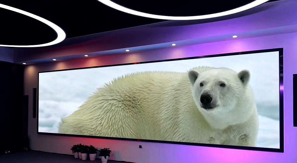
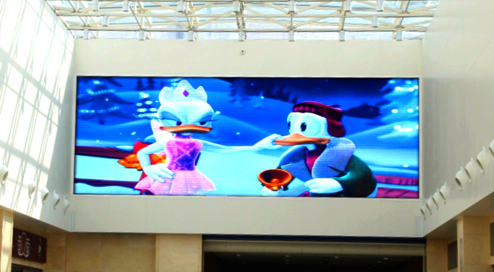
Examples of SMD Packaged Micro-pitch LED Displays
It is with the advantages of mature and stable technology, good heat dissipation effect, convenient maintenance, seamless splicing, low brightness and high gray, etc., SMD package LED display products have been quickly recognized by the market. . Nowadays, LED display screens have been widely used in command rooms, control rooms, conference rooms and other applications. They have been completed in the fields of government emergency command, intelligent command and control, public security traffic police command, general meeting decision-making, energy dispatch center, and military armed police command. A series of high-profile major projects have made the influence of SMD packaged LED displays continue to expand.
COB is a multi-lamp integrated bracket-free packaging technology, which directly encapsulates the light-emitting chip on the PCB board, eliminating the tedious surface mount process. The epoxy resin colloid is tightly and tightly encapsulated in the colloid, without any exposed elements, which provides protection for the LED chip and can solve the problem of damage to the pixels caused by external factors. The pixel failure rate during long-term use is extremely low. Therefore, the COB packaging technology provides ultra-high stability for the micro-pitch LED display without the need to repair the lamp.
In 2013, the first micro-pitch LED high-definition display system was launched to be applied to the forefront of informatization. At the same time, it continued to research and innovate, and devoted itself to researching Micro LED technology and combining COB packaging technology. In 2017, it effectively promoted COB small-pitch LEDs into the field of informatization. The COB package adopts surface-like light emission, so the viewing angle is wider, so that the COB package LED display has a vertical and horizontal two-way 170 ° ultra-wide viewing angle, any angle viewing is a central viewing angle, any angle ensures consistent color and brightness, and has better Optical diffuse color and muddy light effect, the display coverage area is larger, ensuring that there is no dead angle or color cast at any angle, and the image can always be displayed perfectly.
In addition, the COB packaging technology encapsulates the pixels on the PCB board to achieve comprehensive sealing of the PCB circuit board, crystal particles, solder pins and leads. The surface is smooth without exposed components, and the complete protection capability of IP65 is achieved. It has the properties of anti-knock, anti-collision, anti-shock, anti-compression, waterproof, moisture-proof, dust-proof, oil-proof, anti-oxidation, anti-static, etc. It is highly stable and easy to maintain. Daily cleaning and maintenance can directly wipe the surface stains with a damp cloth.
At the same time, the COB packaged micro-pitch LED display adopts a high-quality ultra-black panel, which increases the proportion of black in the entire screen to more than 99%, thereby increasing the contrast ratio of the display to 10,000:1, a qualitative leap. It ensures the color performance of the picture and presents exquisite high-quality images.
Source: Projection Times


Shenzhen LCF Technology Co., Ltd.
Support Hotline
400-618-8884 / 0755-66833488(+86)187-0755-0669
Company Address
LCF Sound & Optoelectronics Industry Park, Gushu, Bao'an District, Shenzhen.
Copyright © 2004-2026 LCF LED Display Screen All rights reserved. Guangdong ICP 15089785-3 Subsidiaries: Dongguan Tongdachuang Industrial Co., Ltd., Anshun Lianshunda Technology Co., Ltd. (holdings)