Publisher: Supplier of LED Display Time: 2021-12-29 14:49 Views: 1789
Compared with other display technologies, LED displays have the advantages of self-illumination, excellent color reproduction, high refresh rate, power saving, and easy maintenance. The two characteristics of high brightness and super-large size can be achieved through splicing are the decisive factors for the rapid growth of led display screens in the past two decades. In the field of large-screen outdoor display, so far no other technology can compete with LED display technology.
However, in the past, LED display screens also had its shortcomings, such as the large spacing between the packaged lamp beads, resulting in low resolution, which is not suitable for indoor and close viewing. In order to improve the resolution, it is necessary to reduce the spacing between the lamp beads, but the size of the lamp beads is reduced. Although the resolution of the entire screen can be improved, the cost will rise rapidly. The excessive cost affects the large-scale commercial application of small-pitch LED displays. .
In recent years, thanks to the efforts of chip manufacturers and packaging manufacturers, IC circuit manufacturers, and screen manufacturers, the cost of single package devices has become lower and lower, LED package devices have become smaller and smaller, and display pixel pitches have become smaller and smaller. The resolution is getting higher and higher, making the advantages of small-pitch LED display in indoor large-screen display more and more obvious.
At present, small-pitch LEDs are mainly used in advertising media, stadiums, stage backgrounds, municipal engineering and other fields, and continue to open up markets in transportation, broadcasting, military and other fields. It is estimated that by 2018, the market size will be close to tens of billions. It can be predicted that in the next few years, the small-pitch LED display will continue to expand its market share and occupy the market space of DLP rear projection. According to the China Everbright Securities Research Institute, by 2020, the replacement rate of small-pitch LED displays for DLP rear projections will reach 70% to 80%.
From the perspective of product design and process technology, the editor will discuss the development of small-pitch LED displays for blue-green LED chips, as well as possible countermeasures on the chip side.

Second, the needs of small-pitch LED displays for LED chips
As the core of the LED display, the LED chip plays a vital role in the development of small-pitch LEDs. The current achievements and future development of small-pitch LED displays rely on unremitting efforts on the chip side.
On the one hand, the dot pitch of the indoor display screen is gradually reduced from the early P4 to P1.5, P1.0, and P0.8 in development. Correspondingly, the lamp bead size has been reduced from 3535 and 2121 to 1010. Some manufacturers have developed 0808 and 0606 sizes, and some manufacturers are even developing 0404 sizes.
As we all know, shrinking the size of packaged lamp beads will inevitably require a reduction in chip size. At present, the surface area of blue-green chips for small-pitch display screens commonly used in the market is about 30 mil2, and some chip factories are already mass-producing chips of 25 mil2 or even 20 mil2.
On the other hand, as the surface area of the chip becomes smaller and the single-core brightness decreases, a series of problems that affect display quality have also become prominent.
The first is the requirement for grayscale. Unlike outdoor screens, the difficulty of indoor screen demand lies not in brightness but in grayscale. At present, the brightness requirement of indoor large-pitch screens is about 1500 cd/m2 -2000 cd/m2, and the brightness of small-pitch LED displays is generally about 600 cd/m2 -800 cd/m2, and the most suitable for long-term attention The best brightness is around 100 cd/m2 -300cd/m2.
One of the current problems with small-pitch LED screens is "low brightness and low gray." That is, the gray scale is not enough at low brightness. To achieve "low brightness and high gray", the current package end adopts a black bracket. Since the black bracket has weak reflection on the chip, the chip is required to have sufficient brightness.
The second is the issue of display uniformity. Compared with conventional screens, the smaller the spacing will cause problems such as afterglow, darker first scan, reddish low brightness, and uneven low gray. At present, in response to problems such as afterglow, first scan dark and low gray and red, both the packaging side and the IC control side have made efforts to effectively alleviate these problems. The uniformity of brightness under low grayscale has also been corrected point by point. Technology has eased. However, as one of the root causes of the problem, more effort is needed on the chip side. Specifically, the uniformity of brightness under small current is better, and the consistency of parasitic capacitance is better.
The third is the reliability issue. The current industry standard is that the allowable value of the LED dead light rate is one in ten thousand, which is obviously not suitable for small-pitch LED displays. Due to the high pixel density of the small-pitch screen and the short viewing distance, if there are 10,000 lights, there will be 1 dead light, and the effect is unacceptable. In the future, the dead-light rate needs to be controlled at one hundred thousandths or even one millionth in order to meet the needs of long-term use.
In general, the development of small-pitch LEDs requires the chip segment to reduce size, increase relative brightness, good brightness consistency under small current, good parasitic capacitance consistency, and high reliability.
Third, the chip-side solution
Size reduction chip size reduction
On the surface, it is the problem of layout design. It seems that it can be solved by designing a smaller layout according to the needs. But can the reduction of chip size go on indefinitely? the answer is negative. There are several reasons that restrict the degree of chip size reduction:
(1) Restrictions on packaging processing. In the packaging process, two factors limit the reduction of chip size. One is the restriction of the nozzle. Die bonding needs to pick up the chip, and the short side of the chip must be larger than the inner diameter of the suction nozzle. There are currently cost-effective nozzles with an inner diameter of about 80um. The second is the limitation of wire bonding. The first is that the wire bonding pad, that is, the chip electrode must be large enough, otherwise the reliability of the wire bonding cannot be guaranteed. The industry reported that the minimum electrode diameter is 45um; secondly, the distance between the electrodes must be large enough, otherwise the two wire bonding will inevitably interfere with each other.
(2) Limitations of chip processing. There are also two limitations in the chip processing process. One is the limitation of the layout. In addition to the limitations of the above-mentioned package end, electrode size and electrode spacing are required, the distance between the electrode and the MESA, the width of the scribe track, and the boundary line spacing of different layers have their limitations, the current characteristics of the chip, the SD process capability, and the processing capability of photolithography. Determine the scope of the specific restrictions. Generally, the minimum distance from the P electrode to the edge of the chip is limited to 14 μm or more.
The second is the limitation of the cutting ability. The SD dicing + mechanical splitting process has its limits, and the chip size may not be split if the chip size is too small. When the diameter of the wafer increases from 2 inches to 4 inches, or to 6 inches in the future, the difficulty of dicing and splitting will increase accordingly, that is, the size of the processable chip will increase accordingly. Taking a 4-inch chip as an example, if the short side length of the chip is less than 90μm and the aspect ratio is greater than 1.5:1, the yield loss will increase significantly.
Based on the above reasons, the author boldly predicts that after the chip size is reduced to 17mil2, the chip design and processing capabilities will be close to the limit, and there is basically no room for reduction, unless there is a major breakthrough in the chip technology program.
2. Brightness increase
Brightness enhancement is an eternal theme on the chip side. The chip factory optimizes the internal quantum effect through the optimization of the epitaxial program, and improves the external quantum effect through the adjustment of the chip structure.
However, on the one hand, the shrinking of the chip size will inevitably lead to the reduction of the area of the light-emitting area, and the brightness of the chip will decrease. On the other hand, the dot pitch of the small-pitch display screen is reduced, and the demand for single-chip brightness is reduced. There is a complementary relationship between the two, but there must be a bottom line. At present, in order to reduce the cost of the chip side, it is mainly to make subtraction on the structure, which usually has to pay the price of reducing the brightness. Therefore, how to weigh the trade-offs is a problem that the industry should pay attention to.
3. Consistency under low current
The so-called small current is relative to the current used by conventional indoor and outdoor chips. The chip I-V curve shown in the figure below, conventional indoor and outdoor chips work in a linear working area, and the current is relatively large. However, small-pitch LED chips need to work in a non-linear working area close to the 0 point, and the current is relatively small.
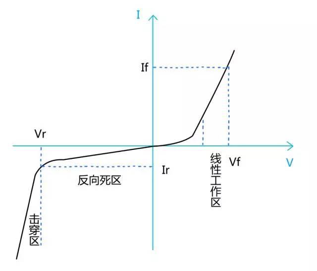
In the non-linear working area, the LED chip is affected by the semiconductor switching threshold, and the difference between the chips is more obvious. Analyzing the discreteness of brightness and wavelength for a large number of chips, it is easy to see that the discreteness of the non-linear working area is much larger than the linear working area. This is an inherent challenge on the chip side at present.
The way to deal with this problem is first to optimize the direction of the extension, mainly to reduce the lower limit of the linear working area; secondly, to optimize the chip spectroscopy to distinguish chips with different characteristics.
4. Parasitic capacitance consistency
At present, there is no condition on the chip side to directly measure the capacitance characteristics of the chip. The relationship between capacitance characteristics and conventional measurement items is still unclear, and those who are waiting for the industry to summarize. The direction of chip-side optimization is firstly the adjustment of the extension, and the other is the refinement of the electrical binning, but the cost is very high and it is not recommended.
5. Reliability
Chip-side reliability can be described by various parameters in the chip packaging and aging process. But in general, the factors affecting the reliability of the chip after it is installed on the screen are mainly ESD and IR.
ESD refers to antistatic ability. According to IC industry reports, more than 50% of chip failures are related to ESD. To improve chip reliability, ESD capabilities must be improved. However, under the condition of the same epitaxial wafer and the same chip structure, the smaller chip size will inevitably lead to the weakening of the ESD capability. This is directly related to the current density and chip capacitance characteristics and cannot be resisted.
IR refers to reverse leakage, and it usually measures the reverse current value of the chip under a fixed reverse voltage. IR reflects the number of defects inside the chip. The larger the IR value, the more defects inside the chip.
To improve ESD capability and IR performance, more optimizations must be made in the epitaxial structure and chip structure. In chip binning, through strict binning standards, chips with weak ESD capability and IR performance can be effectively eliminated, thereby improving the reliability of the chip after it is installed on the screen.
Four, summary
In summary, the editor of Lianchengfa analyzed the series of challenges facing the LED chip end with the development of small-pitch LED displays, and gave improvements or directions one by one. It should be said that there is still a lot of room for the optimization of LED chips. How to improve is still waiting for the industry to use their ingenuity and make continuous efforts.


Shenzhen LCF Technology Co., Ltd.
Support Hotline
400-618-8884 / 0755-66833488(+86)187-0755-0669
Company Address
LCF Sound & Optoelectronics Industry Park, Gushu, Bao'an District, Shenzhen.
Copyright © 2004-2026 LCF LED Display Screen All rights reserved. Guangdong ICP 15089785-3 Subsidiaries: Dongguan Tongdachuang Industrial Co., Ltd., Anshun Lianshunda Technology Co., Ltd. (holdings)