Publisher: Supplier of LED Display Time: 2022-11-28 13:47 Views: 1452
Do you know the several luminance meters commonly used in the LED display industry? Next, Liancheng sent the editor to take a look together!
1. Aiming point luminance meter
Aiming point luminance meter is a photoelectric luminance colorimeter that can choose to measure the field of view. It was first invented by Pritchard. Generally, there are 4 kinds of field of view for switching (2°, 1°, 0.2°, 0.1°). its main structure
as the picture shows:
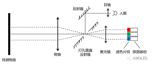
The structure of its optical system is a Kepler telescope structure, which has the characteristics of parallel light incident and parallel light output, including two optical paths, one for visual aiming and one for detection. Wherein the image-space focal point of the objective lens coincides with the object-space focal point of the condenser mirror, and the perforated disk reflector is located here.
When the light beam emitted from the object surface to be measured passes through the perforated disc mirror, most of it is reflected into the visual aiming optical path, and a small part is emitted from the circular hole into the detection optical path. The circular hole of the perforated disk mirror is the field stop of the detection light path, so the circular hole with different apertures can be selected by rotating the perforated disk mirror to realize the switching of the measurement field angle.
When using, first select the measurement field angle, then observe the object surface to be measured through the eyepiece, adjust the focusing ring of the objective lens to focus, and make the field of view clear. At this time, there is a "black hole" in the field of view, which is the round hole of the perforated disc mirror , use the "black hole" to cover the point of the object to be measured to complete the aiming point.
After the aiming point is completed, the measurement can be started. The light beam entering the detection optical path is emitted to the XYZ color filter group after passing through the condenser lens. After being filtered by the XYZ color filter group, the electrical signals generated on the three photodetectors and the object The tristimulus value of the point is proportional to the chromaticity and brightness of the point to be measured.
The aiming-point luminance meter can measure the luminance and chromaticity of a small area on the surface of the object to be measured non-contact at a long distance, and can be used to measure its luminous angle. When measuring flat-panel displays, it is common to measure multiple areas of the screen multiple times to evaluate overall uniformity, and to measure viewing angles by tilting the flat-panel display.
Its main disadvantages are inefficiency in full-screen inspection and poor measurement accuracy in low brightness at small field of view. The picture below shows the BM-7A aiming point luminance meter of Japan TOPCON Company, the luminance range is 0.01-12000000 nit, the luminance accuracy is ±%2, and the color coordinate accuracy is ±0.002.
2. Imaging Luminance Meter
Shortly after the CCD (Charge CoupLED Device) was invented by Bell Laboratories in 1970, its two-dimensional photosensitive ability was applied to digital cameras. The structure of the imaging luminance meter is similar to it. schematic diagram.
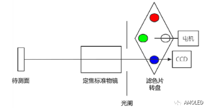
The fixed-focus standard lens images the plane light source to be tested on the CCD photosensitive surface. The diaphragm is responsible for blocking stray light. The motor controls the color filter switching. Three color filters matching the CIE tri-stimulus value curve filter the tri-stimulus value components of the light source. A CCD camera collects images of tristimulus values.
A CCD camera is a two-dimensional image sensor, which consists of a CCD photosensitive chip, a peripheral drive circuit, and an image data processing module. Its core component, CCD, is called a charge-coupled device, and its smallest structural unit is a metal-oxide-semiconductor capacitor (Metal oxide semiconductor, MOS), which uses the photoelectric effect to convert optical signals into electrical signals.
Its workflow is:
1. The peripheral drive circuit exposes the photosensitive surface of the CCD for a certain period of time according to the set parameters.
2. Each photosensitive pixel of CCD generates a corresponding amount of charge according to the amount of light energy received within the exposure time.
3. The peripheral drive circuit controls the transfer of the charge packets in the photosensitive pixel to the adjacent pixels in sequence, and obtains the electrical signal of the entire photosensitive surface by row scanning or column scanning.
4. The image data processing module converts the electrical signal into a standard image transmission format, such as RAW format.
Under the premise of no overexposure, the gray value of each pixel in the obtained image is proportional to the amount of charge accumulated by the corresponding CCD photosensitive pixel during the exposure time. If the image surface illumination distribution remains unchanged during the exposure time, a certain image pixel The relationship between the gray value Fm,n and the illuminance dE of the corresponding image surface element is shown in the formula。

Therefore, the CCD camera can collect the illuminance distribution of the image plane. Under the same photosensitive surface size, the higher the resolution of the CCD camera, the higher the accuracy of the obtained image surface illumination distribution. Usually the resolution of a CCD camera can reach several million pixels, and the resolution of a high-end CCD camera has tens of millions of pixels.
The imaging luminance meter can be approximately equivalent to millions of aiming-point luminance-colorimeters with the same tristimulus value spectral response working at the same time, and each photosensitive pixel unit of the area array CCD camera is equivalent to an aiming-point luminance-colorimeter Integrating photodetectors in a degree meter. The schematic diagram of its microstructure principle is shown in the figure:
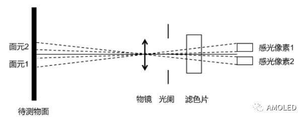
The relationship between the image surface illuminance E and the object surface brightness L is as follows:

Usually, the object distance is far greater than the focal length of the objective lens, and the value of f/l is very small and can be ignored. At this time, the formula can be simplified as:
E=KL
Imaging luminance meters are significantly more efficient than point-and-point luminance meters when measuring the overall brightness and chromaticity distribution of flat panel displays, and are currently the mainstream solution for full-screen inspection of flat panel displays.
In recent years, related machine vision algorithms for screen defect detection have developed rapidly. Some high-end imaging luminance meters also have the function of automatic screen defect detection, which can replace multiple manual detection processes and improve production efficiency and quality management reliability.
For example, the ProMetric imaging colorimeter (as shown in the figure) of Radiant Company in the United States has a brightness range of 0.001-10000000000 nit when equipped with a 50mm standard lens and a 2 million pixel CCD camera, with a brightness accuracy of ±%3 and a color coordinate accuracy of ±0.003. The angle is 10°×8°, and its supporting software TrueTest has the function of defect detection.
3. Spectral brightness meter
The spectrometer can measure the spectrum of the light source and is widely used. In 1992, American scientist Mike Morris invented the first commercial miniature fiber optic spectrometer S1000, which reduced the size of the spectrometer by dozens of times and reduced the price by more than ten times, so that the spectrometer can be used as A module is integrated into the measuring instrument.
A spectrophotometer is a photoelectric luminance colorimeter that uses spectroscopy. The core of its optical system is generally a miniature spectrometer, equipped with a fiber optic probe or incident lens. A commonly used structure of a miniature spectrometer is a crossed Czerny-Turner structure, as shown in the figure:
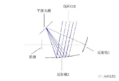
The light beam of the light source is connected to the slit of the micro-spectrometer through fiber coupling, lens focusing, etc. The slit makes the outgoing light a line source, reflected by the mirror 1, and then reaches the plane reflection grating.
Planar reflective gratings are usually made of finely spaced and finely spaced notches on a metal mirror. It is a diffractive optical device with the ability to split light, allowing light of different wavelengths to exit at different diffraction angles.
The mirror 2 focuses light of different wavelengths on different photosensitive pixels of the linear array CCD, and the relative spectral power distribution of the light source can be measured by measuring the electrical signal of each photosensitive pixel. The tristimulus value of the light source can be calculated from the relative spectral power distribution of the light source, thereby calculating the brightness and chromaticity of the light source.
Compared with aiming-point luminance meters and imaging luminance meters, spectral luminance meters have the advantages of high measurement accuracy, compact structure, and measurable spectra. With special fiber optic probes, they can also measure the brightness and chromaticity of pixels. Its main disadvantage is that it can only be measured at a single point.
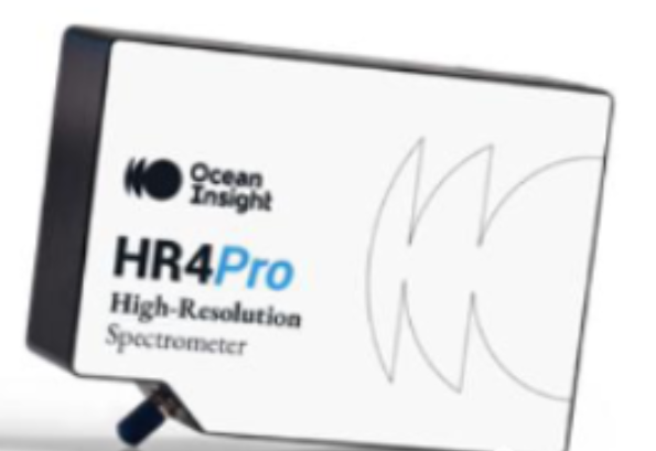
The picture below shows the HR4PRO miniature spectrometer from Ocean Optics, USA. It uses optical fiber to enter the light. Its spectral resolution in the visible light band is 0.1nm, and its size is 148.6 x 104.8 x 45.1 mm, which is close to the size of a smartphone.
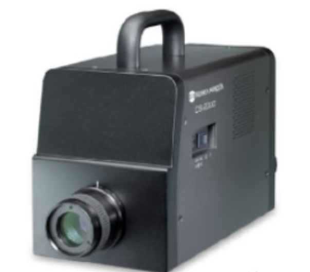
The picture below is the CS2000 spectral luminance meter of Japan Minolta Company, which adopts the lens to enter the light, the field of view angle is 1°, 0.2°, and 0.1° optional, the spectral resolution is 0.9nm, the brightness range is 0.003-500000 nit, and the brightness accuracy is ±% 2. The accuracy of color coordinates is ±0.0015.
4. Microscopic imaging luminance meter
With the improvement of Mini LED and Micro LED display technologies, the demand for measurement of pixel brightness and chromaticity of flat panel displays is increasing. Aim-point photometers, spectral photometers, and imaging photometers are not suitable for quickly measuring pixel brightness and chromaticity of flat panel displays in large quantities.
Among them, the aiming-point luminance meter has a long working distance, and the field of view contains multiple pixels, so it cannot measure a single sub-pixel; the spectral luminance meter needs to be equipped with a special fiber optic probe to measure a single sub-pixel, which cannot be measured in large quantities;
The spatial resolution of the imaging luminance meter is insufficient. It can only measure the pixel luminance and chromaticity of the display panel with a large pixel size, but cannot measure the luminance and chromaticity distribution in the sub-pixel, and cannot measure the pixel luminance and chromaticity of the MiniLED and MicroLED display panels. chroma.
The micro-imaging luminance meter is based on the imaging luminance meter, and the imaging objective lens is replaced by a high-magnification microscopic objective lens. Through high-magnification microscopic imaging, the micron-level brightness and chromaticity distribution measurement of the light source to be measured is realized.
At present, the application scenarios of microscopic imaging luminance meters are relatively single, mainly used for pixel measurement, and have not become a new category. Foreign instrument manufacturers usually launch microscope lens kits and pixel measurement software on the basis of the original imaging luminance meter, so that it can be converted into a microscopic imaging luminance meter by switching lenses.
For example, Radiant's ProMetric imaging colorimeter has launched a 5X microscope lens kit, and its supporting software TrueTest has added a pixel measurement function. At present, no domestic manufacturers have launched microscopic imaging luminance meters.
Source: AMOLED


