Publisher: Supplier of LED Display Time: 2022-09-22 16:31 Views: 3897
OLED was once considered the clear winner for the next generation of high-end TVs. However, LCDs continue to improve and close the performance gap, and new technologies continue to emerge. Among them, MiniLED, MicroLED and QNED have attracted widespread attention as favorable competitors for high-end TV applications.
01 Overview
OLED was once considered the winner of the high-end TV market, but LCD is also becoming more competitive in this area. Technologies such as Quantum Dot (QD), Dual-Cell, Full Array Local Dimming (FALD) backlighting, and MiniLED backlighting have significantly improved LCD performance, while leveraging existing LCD manufacturing lines, and nearly No additional capital expenditure is required. The performance between LCD and OLED is gradually catching up with LCD, but the cost of OLED is still relatively high. As a result, OLED faces increasing competition from LCD in the high-end segment, forcing LG to lower the price of WOLED panels for the first time in years. At the same time, new display technologies and architectures are emerging, including inkjet-printed OLEDs, electroluminescent QDs, QD-OLEDs, MicroLEDs, QNEDs. Committed to developing the next generation of high-end display technologies and products, Samsung also finally decided to shut down all of its LCD production lines.
02 MiniLED
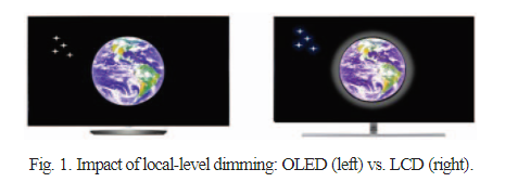
If the number of partitions is increased to more than 5,000 and the number of LEDs exceeds 10,000, MiniLED can further enable more viewers to experience image quality close to OLED, or imperceptible difference. In addition, MiniLED reduces power consumption by up to 50% compared to traditional LCD and enables brightness adjustment significantly better than OLED.
Architecture
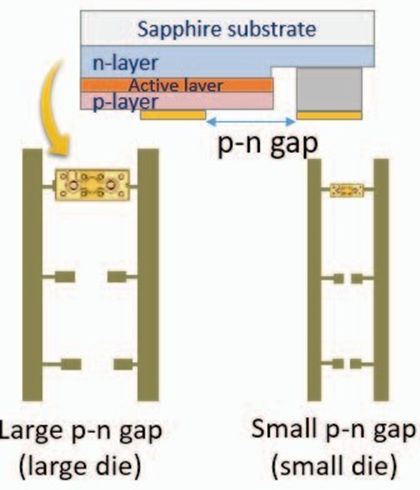
The design of MiniLED backlights involves complex trade-offs between performance, cost, and appearance (thickness). LED Chip size and quantity will affect brightness, thickness, contrast, cost and mass producibility. The choice of substrate is also influenced by cost, mass production and chip size: as the chip size decreases, the gap between the N-pad and P-pad decreases. This requires stricter PCB specifications: flatness, roughness, etc. to ensure precise die bonding requirements.
It is also a huge workload to bond tens of thousands of Mini LEDs. Standard LED chip punching equipment cannot provide sufficient placement accuracy and capacity sales. Therefore, a new generation of die bonding equipment is required. High-precision die bonders also typically work in relatively small work areas. As the size of TVs increases, now usually reaching 65", 75" or above, MiniLED backlight panels must be assembled in a modular splicing manner. For the PCB, the electrical connections are linked through board traces to the back of the PCB where the driver IC and other components are located. PCB boards can have multiple layers to allow complex routing of signals and enable seamless, gap-free assembly. For glass panels, module splicing becomes an issue because signals need to be routed to the edge of the glass panel using flexible edge connectors bonded to the glass surface.
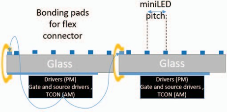
Through vias (aka "TGV" for through glass vias) are still prohibitively expensive. As the pitch decreases, the area that can be used to bond and bend flexible connectors without creating pitch discontinuities decreases. Flexible connectors are currently the preferred choice, although some panel manufacturers have developed edge connectors that are deposited directly on the edge of the glass.
drive
Passive Matrix (PM) is the standard for LCD FALD backlights. It's great for displays with fewer partitions. However, when the number of partitions increases to more than a few thousand, the PM drive performance decreases and the number of driver ICs increases, resulting in an increase in cost.
Active matrix (AM) MiniLED backlight driving can be achieved using a glass-based thin film transistor (TFT) backplane. However, the high currents required to drive the LED chips require special TFT designs that require large channels. Alternatively, the TFT can only provide switching transistors, and the driving transistors are provided as discrete MOSFET circuits, which are assembled in the same way as a scaled wafer, with a discrete CMOS circuit providing full drive and compensation transistors and capacitors. The concept of "Minidriver" is shown in the figure below.
03 MicroLED
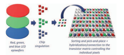
MicroLED displays use individual, small LED Chips as subpixels. Unlike OLEDs, LED Chips require high processing temperatures (>1 000°C) and cannot be "grown" and patterned directly on transistor matrices. As a result, MicroLED wafers need to now be fabricated on 4-inch to 12-inch wafers, singulated, transferred and assembled to display substrates. That is, RGB display can be realized from a single red, green, and blue LED chip, or a blue LED chip combined with red and green quantum dots can be used to convert into white light.
As a self-luminous technology, MicroLED retains all the advantages of OLED: pixel-level dimming, wide viewing angle, etc. It can also provide higher brightness. As a stable inorganic material, MicroLED is stable and durable, eliminating the go-to point of OLED: the risk of afterimages and the need for complex and expensive packaging.
For TV applications in particular, MicroLEDs also offer a unique feature: since they do not require sealing like LCDs or encapsulation like OLEDs, MicroLEDs can be 100% bezel-less. The seamless splicing of MicroLED modules allows the construction of displays of any size (as shown below).
This modular design improves manufacturing yields and can significantly reduce the cost of large displays, simplifying the shipping, delivery and installation of "giant" TVs over 100 sizes.
challenge
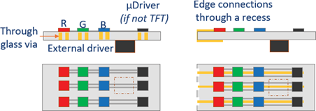
MicroLED displays face many challenges, including assembly, efficiency of small microLEDs, driving, yield, and rework repairs. The splicing of MicroLED modules presents additional challenges. The modules must be borderless, stitched and assembled absolutely flawlessly, both mechanically and with the calibration of each module (color, brightness, contrast...). Signals and power must be routed from the back of the module to the pixels, either through glass through vias ("TGVs") or through the edge of each module, as shown in the diagram below.
Various techniques and architectures are currently being explored to enable signal routing from the front of the module to the back. These include TGVs, surrounding electrodes, flexible TFT backplanes.
04 QNED
"QNED" stands for "Quantum Nano-Emitting Diodes". QNEDs were jointly developed by Korea University, PSI and Samsung.
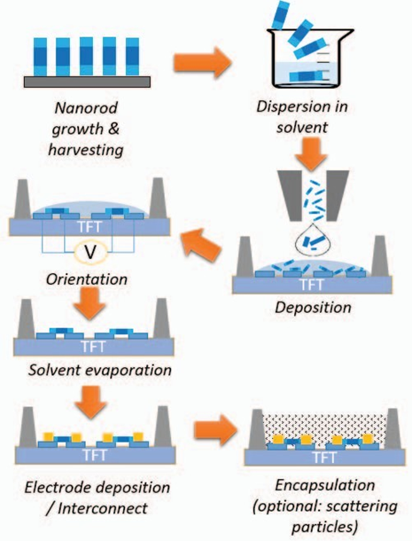
QNEDs consist of micron to nanoscale LED "rods", typically 2-3 microns long and 0.5 microns in diameter, that self-assemble. Rod-shaped μLEDs are grown, harvested, coated with surfactants to avoid aggregation and dispersed into solvents. The μLED "solution" is deposited on the TFT backplane by inkjet printing, with pixels separated by "dams".
Electrodes on the pixel groups are used to apply asymmetric AC voltages (typically 0-30V at 950 kHz). This creates a force that aligns the "rod" perpendicular to the electrodes, which then evaporates the solvent and deposits the connecting electrodes. Finally, scattering particles and color conversion (QD materials) are added and encapsulated, as shown in the figure below.
Potential benefits
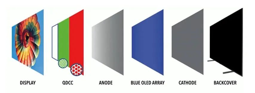
QNED display structure and fabrication process are similar to QD-OLED. QNEDs can address some of the major challenges associated with QD-OLEDs by replacing multi-layer stacks of fragile, low-efficiency, blue OLED materials with stable, long-life, high-efficiency inorganic "coatings" of QNEDs.
The QNEDs were self-assembled using ink jet printing (IJP). IJP is already used in the production of OLED packages. Many companies are working on IJPs for RGB OLED subpixels. Samsung will use it to deposit patterned QD conversion layers in its QD-OLEDs. Each QNED pixel contains 10x to several 10's of QNEDs. This margin is good for yield and repair, compared to Micro LED.
challenge
Just like MicroLED or QD-OLED, QNED technology has not yet been proven in volume manufacturing. Many potential challenges may remain major obstacles. To provide good performance and brightness, the external efficiency (EQE) of the nanorods should be at least comparable to current commercial blue OLED materials, i.e. >6%. Since they can withstand higher driving conditions than OLEDs, they can deliver higher brightness even at similar efficiencies.
But the nanorods are etched vertically through the epilayer. Just like standard μLEDs, etching creates surface defects that significantly reduce internal efficiency. Such solid, nano-sized LED rods, inkjet-printed deposition may present various challenges, such as printer nozzle clogging, aggregation, non-uniform repartitioning in pixel banks (“coffee ring” effect), etc. The process must also ensure that enough QNEDs are lit in each pixel to control the pixel/pixel variation within a range that can be compensated by driving. Typically, only 60-80% of QNEDs are operational after assembly.
For cost reasons, the number of QNEDs per subpixel cannot exceed a few 10s, so it must be ensured that this will result in enough "bars" to light up in each pixel to meet the brightness requirements.
05 Conclusion
The TV industry is at a crossroads where LCDs dominate, but there is little opportunity for differentiation after production lines are built.
MiniLED backlight technology, which can use existing LCD production lines, requires little investment, and enhances the value of panels with backlighting.
MicroLEDs have specific advantages, enabling modular displays or any arbitrary size. However, major manufacturing hurdles remain.
By addressing some of the major challenges associated with OLED and MicroLED technology, QNEDs could open a third path between OLED and MicroLED. However, they have not yet been demonstrated in mass production, and some fundamental challenges remain.
At the same time, OLED continues to improve in the trade-off between cost and performance. Most OLED panel makers are actively working on inkjet-printed RGB OLEDs and electroluminescent QDs, which, if successful, could also win the battle for next-generation high-end TVs.
Source: MiniLED Industry Network
