Publisher: Supplier of LED Display Time: 2022-09-19 18:00 Views: 1710
High-power LED packaging has been a research hotspot in recent years due to its complex structure and process, which directly affects the performance and life of LEDs, especially high-power white LED packaging.
The functions of the LED package mainly include: 1. Mechanical protection to improve reliability;
2. Strengthen heat dissipation to reduce wafer junction temperature and improve LED performance;
3. Optical control, improve light output efficiency and optimize beam distribution;
4. Power supply management, including AC/DC conversion, and power control.
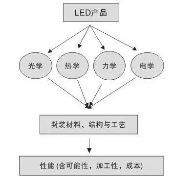
The selection of LED packaging methods, materials, structures and processes is mainly determined by factors such as wafer structure, optoelectronic/mechanical properties, specific applications, and cost. After more than 40 years of development, LED packaging has gone through development stages such as bracket type (Lamp LED), SMD type (SMD LED), and bare core type LED (COB LED).
Key technologies of high-power LED packaging
High-power LED packaging mainly involves light, heat, electricity, structure and technology. These factors are both independent of each other and affect each other. Among them, light is the purpose of LED packaging, heat is the key, electricity, structure and technology are the means, and performance is the specific embodiment of the packaging level. In terms of process compatibility and reducing production costs, LED package design should be carried out at the same time as chip design, that is, the package structure and process should be considered during chip design. Otherwise, after the wafer fabrication is completed, the structure of the wafer may be adjusted due to packaging requirements, thereby prolonging the product development cycle and process cost, and sometimes even impossible.
Low thermal resistance packaging process
For the existing LED light efficiency level, since about 80% of the input electrical energy is converted into heat, and the LED chip area is small, the chip heat dissipation is a key problem that must be solved in LED packaging. It mainly includes chip layout, packaging material selection (substrate material, thermal interface material) and process, heat sink design, etc.
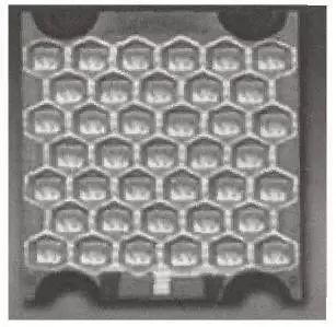
LED package thermal resistance mainly includes internal thermal resistance and interface thermal resistance of materials (heat dissipation substrate and heat sink structure). The function of the heat dissipation substrate is to attract the heat generated by the wafer and conduct it to the heat sink to achieve heat exchange with the outside world. Commonly used heat dissipation substrate materials include silicon, metals (such as aluminum, copper), ceramics (such as Al2O3, AIN, Sic), and composite materials. For example, Nichia's third-generation LED uses CuW as the substrate, and flip-chips a 1mm chip on the CuW substrate, which reduces the thermal resistance of the package and improves the luminous power and efficiency; Lamina Ceramics has developed a low-temperature co-fired ceramic metal substrate. , and developed the corresponding LED packaging technology. This technology firstly prepares a high-power LED chip and a corresponding ceramic substrate suitable for eutectic welding, and then directly welds the LED chip and the substrate together. Because the eutectic solder layer, electrostatic protection circuit, driving circuit and control compensation circuit are integrated on the substrate, it is not only simple in structure, but also has a high thermal conductivity of the material and few thermal interfaces, which greatly improves the heat dissipation performance, which is a high-power LED array package. A solution is proposed. The high thermal conductivity copper clad ceramic board developed by German Curmilk company is made of ceramic substrate (AIN and Al2O3) and conductive layer (Cu) sintered under high temperature and high pressure. No binder is used, so it has good thermal conductivity, high strength and insulation. powerful. Among them, the thermal conductivity of aluminum nitride (AIN) is 160W/mk, and the thermal expansion coefficient is 4.0×10⁻⁶/℃ (equivalent to the thermal expansion coefficient of silicon, which is 3.2×10⁻⁶/℃), thereby reducing the thermal stress of the package.
The article is excerpted from Internet resources. If there is any infringement, please contact us to delete it in time.


 and Virtual Reality (VR)?")


Shenzhen LCF Technology Co., Ltd.
Support Hotline
400-618-8884 / 0755-66833488(+86)187-0755-0669
Company Address
LCF Sound & Optoelectronics Industry Park, Gushu, Bao'an District, Shenzhen.
Copyright © 2004-2026 LCF LED Display Screen All rights reserved. Guangdong ICP 15089785-3 Subsidiaries: Dongguan Tongdachuang Industrial Co., Ltd., Anshun Lianshunda Technology Co., Ltd. (holdings)